| Item | Content |
|---|---|
| Product No. | RP01A-RK3588S |
| Version | V1.0 |
| Release Date | Jan. 28, 2026 |
| Effective Date | Jan. 28, 2026 |
| Document Status | Under Revision |
| Compiled by | Wang Zhihai |
| Reviewed by | |
| Confidentiality Level | Public |
| Version | Release Date | Upgrade Record |
|---|---|---|
| V1.0 | Jan. 28, 2026 | First release |
1. Interface Schematic Diagram
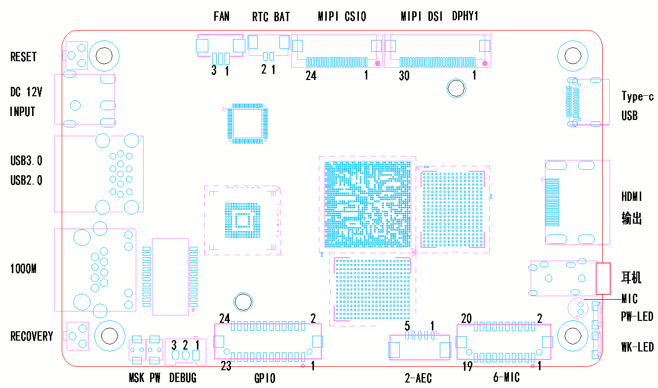
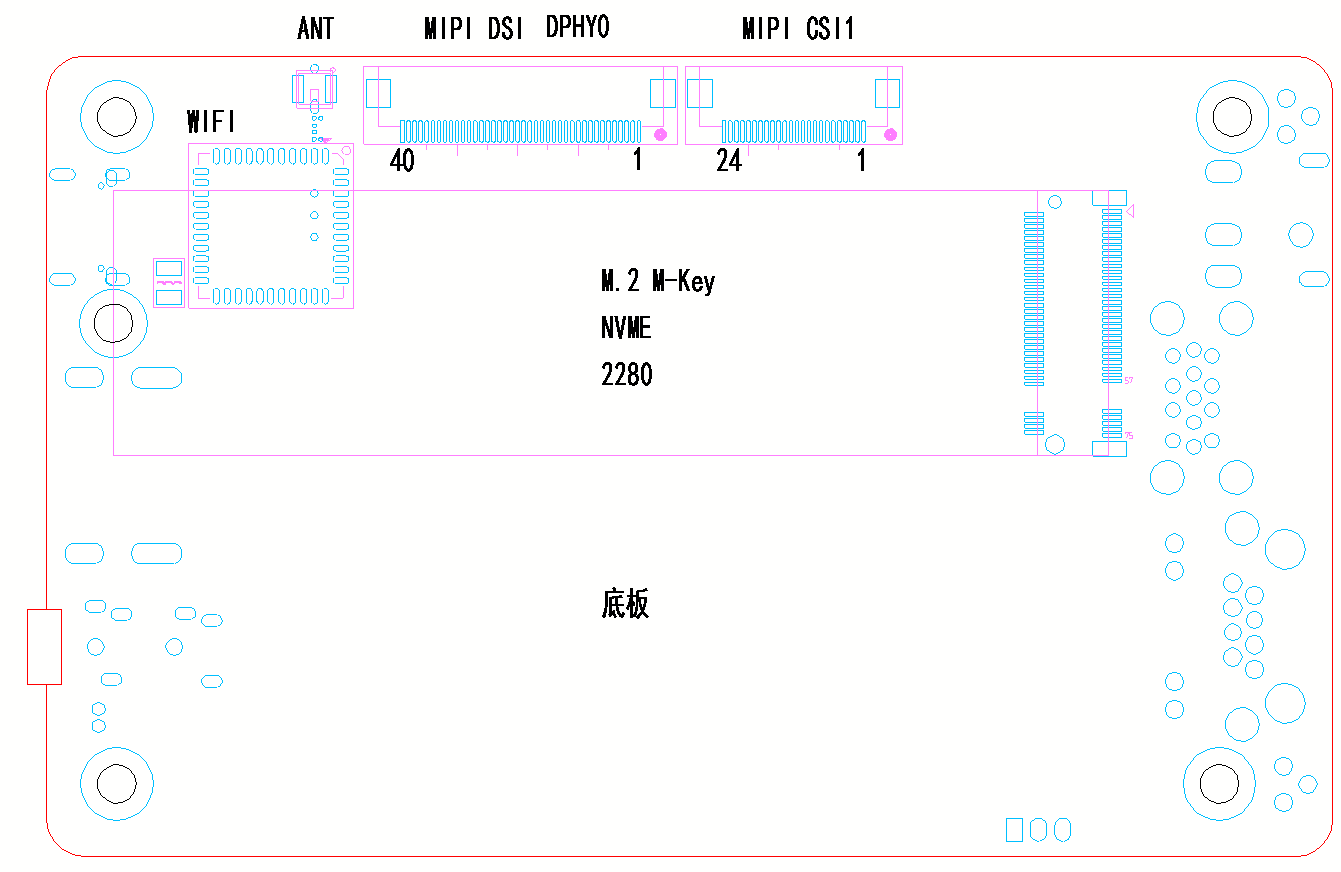
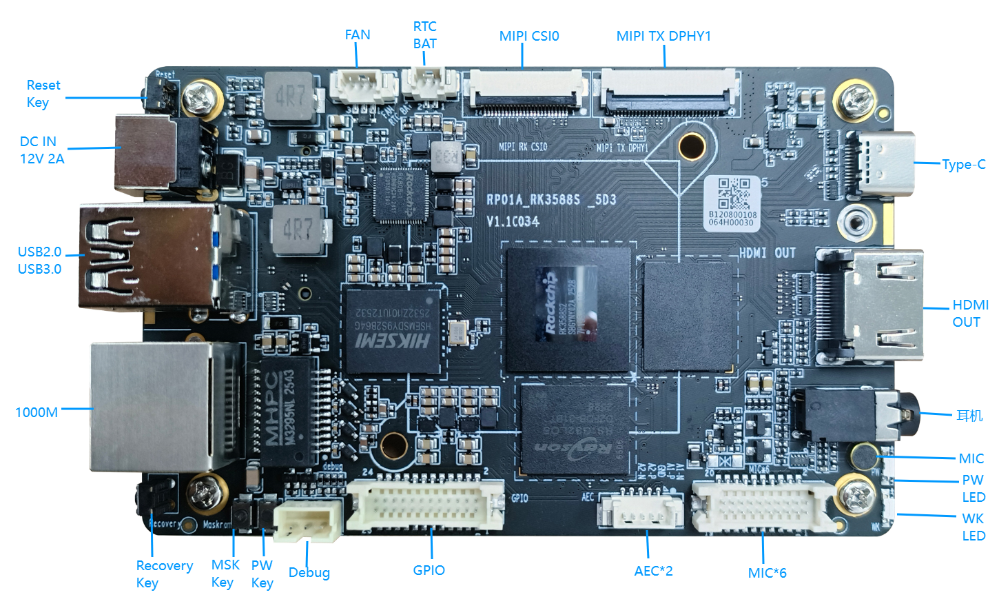
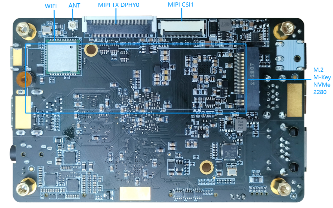
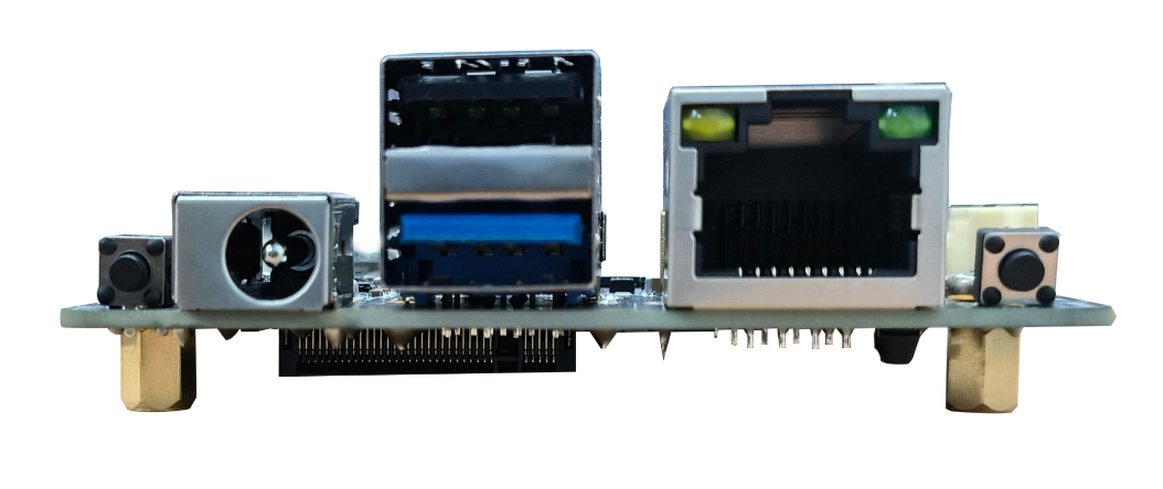
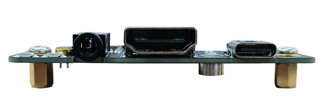
2. Port Description
1. Debug Port
Baud Rate: 1500000bps
Voltage Level: 3.3V
Connector Specification: 2.0MM 3P
| Pin Definition of RP01-RK3588S2 Debug Port | ||
| Pin No. | Pin Definition | Description |
| 1 | RXD | Serial Receive |
| 2 | TXD | Serial Transmit |
| 3 | GND | Power Ground |
2. Recovery Key
The Recovery key is mainly used to enter Recovery mode for EMMC image flashing and downloading.
Operation steps: Open Rockchip Development Tool. With the power off, connect the data cable to the Type-C OTG port. Keep pressing the Recovery key, then connect the 12V power supply. Release the key once the tool detects the Recovery device, and proceed with image flashing.
Refer to the firmware flashing chapter for details.
3. Maskrom Key
The Maskrom key is used to enter MaskRom mode to flash and download images to EMMC. It is applicable for firmware corruption and system boot failure scenarios.
Operation steps: Open Rockchip Development Tool. With the power off, insert the data cable into the Type-C OTG port. Hold down the Maskrom key and connect the 12V power supply. Release the key when the tool recognizes the MaskRom device, then start image flashing.
See Chapter 5 for firmware flashing instructions.
4. Power Key
It serves as system power on/off and sleep key.
- Under Linux system: used for system power on and power off.
- Under Android system: used for system sleep function.
5. Reset Key
It is designed for system reset and reboot. Pressing this key under any status will trigger power-off restart of the system.
6. GPIO Port
Adopt 1.25MM 2*12P board-to-wafer connector. Pin definitions are listed as follows.
Note: Ensure consistent port voltage level during use. Different voltage levels may cause CPU damage.
| RP01-RK3588S2 GPIO Pin Definition | ||||||
|---|---|---|---|---|---|---|
| Pin | Voltage Level | GPIO | Function 1 | Function 2 | Function 3 | Function 4 |
| 1 | 3V3 | |||||
| 3 | 3V3 | |||||
| 5 | GND | |||||
| 7 | GND | |||||
| 9 | 3.3V | GPIO1_B7 | UART1_RX_M1 | I2C5_SDA_M3 | SPDIF1_TX_M0 | PWM13_M2 |
| 11 | 3.3V | GPIO1_B6 | UART1_TX_M1 | I2C5_SCL_M3 | SPDIF0_TX_M0 | MIPI_CAM1_CLK_M0 |
| 13 | 3.3V | GPIO1_B5 | UART7_TX_M2 | SPI0_CS1_M2 | ||
| 15 | 3.3V | GPIO1_B4 | UART7_RX_M2 | SPI0_CS0_M2 | ||
| 17 | 3.3V | GPIO4_B2 | PWM14_M1 | I2S1_SDO2 | ||
| 19 | 3.3V | GPIO4_B5 | PWM12_M1 | |||
| 21 | 3.3V | GPIO4_A3 | UART0_TX_M2 | |||
| 23 | 3.3V | GPIO4_A4 | UART0_RX_M2 | |||
| 2 | 5V0 | |||||
| 4 | 5V0 | |||||
| 6 | GND | |||||
| 8 | GND | |||||
| 10 | 3.3V | GPIO1_C1 | UART3_TX_M0 | I2C3_SCL_M0 | SPI4_MISO_M0 | |
| 12 | 3.3V | GPIO1_C0 | UART3_RX_M0 | I2C3_SDA_M0 | SPI4_MOSI_M0 | |
| 14 | PWRON_L | |||||
| 16 | 1.8V | GPIO1_C4 | PWM11_IR_M2 | SPI4_CS0_M0 | ||
| 18 | 1.8V | GPIO1_C6 | PWM15_IR_M2 | |||
| 20 | 1.8V | GPIO0_A4 | ||||
| 22 | 1.8V | GPIO0_D3 | ||||
| 24 | 1.8V | GPIO0_D5 |
7. 6-MIC Input Port
The 6-MIC input port adopts 1.25MM 2*10P board-to-wire wafer connector. The interface definitions are as follows:
| RP01-RK3588S2 6-MIC Input Pin Definition | |||||
|---|---|---|---|---|---|
| Pin No. | Pin Definition | Description | Pin No. | Pin Definition | Description |
| 1 | MIC1+ | MIC1 Positive | 2 | MIC2+ | MIC2 Positive |
| 3 | MIC1- | MIC1 Negative | 4 | MIC2- | MIC2 Negative |
| 5 | AGND | Analog Ground | 6 | AGND | Analog Ground |
| 7 | MIC3+ | MIC3 Positive | 8 | MIC4+ | MIC4 Positive |
| 9 | MIC3- | MIC3 Negative | 10 | MIC4- | MIC4 Negative |
| 11 | AGND | Analog Ground | 12 | AGND | Analog Ground |
| 13 | MIC5+ | MIC5 Positive | 14 | MIC6+ | MIC6 Positive |
| 15 | MIC5- | MIC5 Negative | 16 | MIC6- | MIC6 Negative |
| 17 | AGND | Analog Ground | 18 | AGND | Analog Ground |
| 19 | MIC3V3 | MIC Power Supply | 20 | AGND | Analog Ground |
8. 2-AEC Input Port
The 2-AEC input port is mainly used for external sound feedback collection to realize echo cancellation sampling. It adopts 1.25MM 1*5P board-to-wire wafer connector. The interface definitions are as follows:
| RP01-RK3588S2 2-AEC Input Pin Definition | ||
|---|---|---|
| Pin No. | Pin Definition | Description |
| 1 | AEC1_N | Speaker L Negative |
| 2 | AEC1_P | Speaker L Positive |
| 3 | AGND | Analog Ground |
| 4 | AEC2_P | Speaker R Positive |
| 5 | AEC2_N | Speaker R Negative |
AEC Echo Acquisition Block Diagram
image-2026-1-28_17-7-10.png
9. Headphone Interface
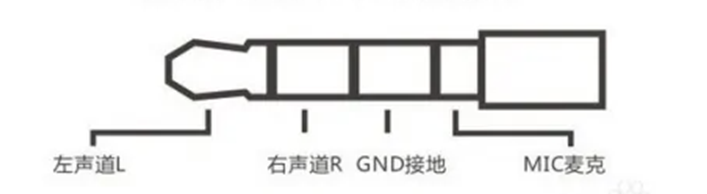
It integrates ES8388 audio codec, supporting audio output and microphone input. The microphone signal is connected to the IN1 channel of ES8388. It adopts standard 3.5mm 4-pole international audio jack.
Headphone Insertion Detection:HP_DET --- GPIO1_D5--- High level "1" for headphone inserted; Low level "0" for headphone removed.
Headphone Output Control:EAR_CTL --- GPIO1_D2---Output "1" to enable headphone output; Output "0" to disable headphone output.
10. Built-in MIC
Adopts 4020 capacitive microphone, which is connected to the IN2 channel of ES8388.
Simple voice interaction can be realized through dedicated algorithms.
11. MIPI DSI DPHY1 Interface
This interface uses 0.5MM 30P FPC connector with bidirectional contact design.
It is equipped with 4-lane DPHY, supporting maximum bandwidth up to 4.5Gbps. Combined with MIPI DSI DPHY0, it can realize 4K resolution output.
External conversion IC can be used to convert MIPI signal to LVDS output.
| RP01-RK3588S2 MIPI DSI DPHY1 Pin Definition | ||
|---|---|---|
| Pin No. | Pin Definition | Description |
| 1 | GND | Power Ground |
| 2 | DPHY1_TX_D0N | DPHY1 Data 0 Negative |
| 3 | DPHY1_TX_D0P | DPHY1 Data 0 Positive |
| 4 | GND | Power Ground |
| 5 | DPHY1_TX_D1N | DPHY1 Data 1 Negative |
| 6 | DPHY1_TX_D1P | DPHY1 Data 1 Positive |
| 7 | GND | Power Ground |
| 8 | DPHY1_TX_CLKN | DPHY1 Clock Negative |
| 9 | DPHY1_TX_CLKP | DPHY1 Clock Positive |
| 10 | GND | Power Ground |
| 11 | DPHY1_TX_D2N | DPHY1 Data 2 Negative |
| 12 | DPHY1_TX_D2P | DPHY1 Data 2 Positive |
| 13 | GND | Power Ground |
| 14 | DPHY1_TX_D3N | DPHY1 Data 3 Negative |
| 15 | DPHY1_TX_D3P | DPHY1 Data 3 Positive |
| 16 | GND | Power Ground |
| 17 | MIPI_BL_PWM2 | Display backlight PWM signal output, GPIO0_C4 PWM2_0, 1.8V level |
| 18 | MIPI_TE2 | Display TE signal output, leave floating when unused, GPIO1_B0, 1.8V level |
| 19 | LCD3V3 | 3.3V power supply for display |
| 20 | LCD_RST2 | Display reset pin output, GPIO1_B3, 3.3V level |
| 21 | LCD_ID | Display ID pin, pulled low by default |
| 22 | LCD_EN | Display enable pin, pulled high by default, 3.3V output |
| 23 | TP_SCL | Reserved touch I2C SCL, 3.3V level (shared with DPHY0) |
| 24 | TP_SDA | Reserved touch I2C SDA, 3.3V level (shared with DPHY0) |
| 25 | TP_INT | Reserved touch interrupt input, 3.3V level (shared with DPHY0) |
| 26 | TP_RST | Reserved touch reset output, 3.3V level (shared with DPHY0) |
| 27 | GND | Power Ground |
| 28-30 | LCD5V0 | 5V power output |
12. MIPI CSI0 Interface
This interface uses 0.5MM 24P FPC connector, which supports double-sided insertion.
It is configured with 4-lane DPHY, with bandwidth of 2.5Gbps per lane. When used together with CSI1, it supports 8K@15FPS video input.
| RP01-RK3588S2 MIPI CSI0 Pin Definition | ||
|---|---|---|
| Pin No. | Pin Definition | Description |
| 1 | I2C7_SDA_M0 | I2C7_SDA_M0, 1.8V level |
| 2 | I2C7_SCL_M0 | I2C7_SCL_M0, 1.8V level |
| 3 | GND | Power Ground |
| 4 | MIPI_CAM1_PDN_L | Camera power enable output, GPIO3_C1, 1.8V level |
| 5 | MIPI_CAM1_RST_L | Camera reset output, GPIO3_C1, 1.8V level |
| 6 | GND | Power Ground |
| 7 | MIPI_CSI0_RX_CLKN | CSI0 clock negative |
| 8 | MIPI_CSI0_RX_CLKP | CSI0 clock positive |
| 9 | GND | Power Ground |
| 10 | MIPI_CLKOUT | Camera reference clock output |
| 11 | GND | Power Ground |
| 12 | MIPI_CSI0_RX_D0N | CSI0 data 0 negative |
| 13 | MIPI_CSI0_RX_D0P | CSI0 data 0 positive |
| 14 | MIPI_CSI0_RX_D1N | CSI0 data 1 negative |
| 15 | MIPI_CSI0_RX_D1P | CSI0 data 1 positive |
| 16 | GND | Power Ground |
| 17 | MIPI_CSI0_RX_D2N | CSI0 data 2 negative |
| 18 | MIPI_CSI0_RX_D2P | CSI0 data 2 positive |
| 19 | MIPI_CSI0_RX_D3N | CSI0 data 3 negative |
| 20 | MIPI_CSI0_RX_D3P | CSI0 data 3 positive |
| 21 | GND | Ground |
| 22-24 | VCC3V3 | 3.3V power output for camera |
Since this board is compatible with both RK3588S and RK3588S2 chips, the only difference lies in the MIPI RX interface. Users only need to adjust the RX link configuration in software.
The link comparison is shown as follows:
| Board Marking | RK3588S | RK3588S2 | Picture |
|---|---|---|---|
| MIPI SCI0 J2600 | MIPI D/C-PHY CSI_RX PORT0 1*4lane | MIPI DPHY CSI_RX PORT0 1*4lane | image-2026-4-3_18-40-37.png |
| MIPI SCI0 J9906 | MIPI DPHY CSI_RX PORT0 1*4lane | MIPI DPHY CSI_RX PORT1 1*4lane | image-2026-4-3_18-41-31.png |
13. MIPI DSI DPHY0 Interface
This interface uses 0.5mm 40P FPC connector which supports double-sided connection.
It adopts 4-lane DPHY with a maximum bandwidth of 4.5Gbps, featuring backlight output and touch input functions. Combined with MIPI DSI DPHY1, it can output 4K resolution display signal.
| RP01-RK3588S2 MIPI DSI DPHY0 Pin Definition | ||
|---|---|---|
| Pin No. | Pin Definition | Description |
| 1 | NC | No Connection |
| 2 | VCC | 3.3V power supply for display |
| 3 | IOVCC | 3.3V display IO power supply |
| 4 | GND | Power Ground |
| 5 | RESET | Display reset, GPIO1_B1, 3.3V level |
| 6 | NC | No Connection |
| 7 | GND | Power Ground |
| 8 | DPHY0_TX_D0N | DPHY0 Data 0 Negative |
| 9 | DPHY0_TX_D0P | DPHY0 Data 0 Positive |
| 10 | GND | Power Ground |
| 11 | DPHY0_TX_D1N | DPHY0 Data 1 Negative |
| 12 | DPHY0_TX_D1P | DPHY0 Data 1 Positive |
| 13 | GND | Power Ground |
| 14 | DPHY0_TX_CLKN | DPHY0 Clock Negative |
| 15 | DPHY0_TX_CLKP | DPHY0 Clock Positive |
| 16 | GND | Power Ground |
| 17 | DPHY0_TX_D2N | DPHY0 Data 2 Negative |
| 18 | DPHY0_TX_D2P | DPHY0 Data 2 Positive |
| 19 | GND | Power Ground |
| 20 | DPHY0_TX_D3N | DPHY0 Data 3 Negative |
| 21 | DPHY0_TX_D3P | DPHY0 Data 3 Positive |
| 22 | GND | Power Ground |
| 23 | TP_VCC | 3.3V touch power supply |
| 24 | TP_VCC | 3.3V touch power supply |
| 25 | GND | Power Ground |
| 26 | TP_SDA | Touch I2C SDA, 3.3V level |
| 27 | TP_SCL | Touch I2C SCL, 3.3V level |
| 28 | TP_RST | Touch reset output, 3.3V level |
| 29 | TP_INT | Touch interrupt input, 3.3V level |
| 31-32 | LED_BL- | Display backlight negative pole, current sampling pin |
| 33-38 | NC | No Connection |
| 39-40 | LED_BL+ | Display backlight positive pole, output 15-28V@50mA |
14. MIPI CSI1 Interface
This interface adopts 0.5mm 24P FPC connector with double-sided pluggable design.
It is equipped with 4-lane DPHY with 2.5Gbps bandwidth per lane. Combined with CSI0, it supports 8K@15FPS video input.
| RP01-RK3588S2 MIPI CSI1 Pin Definition | ||
|---|---|---|
| Pin No. | Pin Definition | Description |
| 1 | I2C2_SDA_M0 | I2C2_SDA_M0, 1.8V level |
| 2 | I2C2_SCL_M0 | I2C2_SCL_M0, 1.8V level |
| 3 | GND | Power Ground |
| 4 | MIPI_CAM2_PDN_L | Camera power enable output, GPIO3_C6, 1.8V level |
| 5 | MIPI_CAM2_RST_L | Camera reset output, GPIO1_A6, 1.8V level |
| 6 | GND | Power Ground |
| 7 | MIPI_CSI1_RX_CLKN | CSI1 clock negative |
| 8 | MIPI_CSI1_RX_CLKP | CSI1 clock positive |
| 9 | GND | Power Ground |
| 10 | MIPI_CLKOUT | Camera reference clock output |
| 11 | GND | Power Ground |
| 12 | MIPI_CSI1_RX_D0N | CSI1 data 0 negative |
| 13 | MIPI_CSI1_RX_D0P | CSI1 data 0 positive |
| 14 | MIPI_CSI1_RX_D1N | CSI1 data 1 negative |
| 15 | MIPI_CSI1_RX_D1P | CSI1 data 1 positive |
| 16 | GND | Power Ground |
| 17 | MIPI_CSI1_RX_D2N | CSI1 data 2 negative |
| 18 | MIPI_CSI1_RX_D2P | CSI1 data 2 positive |
| 19 | MIPI_CSI1_RX_D3N | CSI1 data 3 negative |
| 20 | MIPI_CSI1_RX_D3P | CSI1 data 3 positive |
| 21 | GND | Ground |
| 22-24 | VCC3V3 | 3.3V power output for camera |
15. Fan Interface
It is a fan interface with PWM output. The fan will automatically turn on when the temperature exceeds the set threshold.
Equipped with 1.25mm 3P connector.
| RP01-RK3588S2 Fan Interface Pin Definition | ||
|---|---|---|
| Pin No. | Pin Definition | Description |
| 1 | GND | Power Ground |
| 2 | FAN_PWM | Fan PWM signal, 5V level |
| 3 | VCC_FAN | Fan power supply, default 5V output, switchable to 12V |
16. M.2 M-Key PCIE2.0
M.2 M-Key interface supports external 2280-size NVMe SSD. Adopts PCIE2.0 x1 lane with 5Gbps bandwidth, compatible with mainstream commercial SSDs.
17. Ethernet
Led out via RJ45 connector, supports 10/100/1000Mbps transmission rate.
18. Type-C USB
Supports USB3.0 OTG for firmware burning, and DP1.4a video output up to 4K@60Hz.
19. USB3.0 & USB2.0
1 channel Type-A USB3.1 Gen1 Host, speed up to 5Gbps.
1 channel Type-A USB2.0 Host, speed up to 480Mbps.
Total combined output current reaches 1A.
20. HDMI Output
Adopts HDMI2.1 Type-A connector, maximum output up to 8K@60Hz.
21. RTC
Onboard RTC interface, used for connecting 2Pin 1.25mm RTC backup battery.
22. Power Input Interface
12V 2A DC power input, 5.5*2.0 standard DC jack.