| Item | Content |
|---|---|
| Product No. | EDGE-RK3576 |
| Version | V1.0 |
| Release Date | 2026-04-10 |
| Effective Date | 2026-04-10 |
| Document Status | Under Revision |
| Prepared by | Wang Zhihai |
| Reviewed by | |
| Confidentiality Level | Public |
| Version | Release Date | Update Record |
|---|---|---|
| V1.0 | 2026-04-10 | First release |
1. Interface Diagram
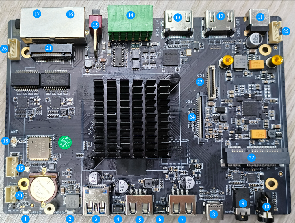
| NO. | Description | NO. | Description |
|---|---|---|---|
| 1 | Power indicator | 14 | RS485, RS232, GPIO & 12V power output |
| 2 | Activity indicator | 15 | GPIO input level polarity DIP switch |
| 3 | USB 3.0 port | 16 | RJ45 |
| 4 | Upgrade key | 17 | RJ45 |
| 5 | USB 2.0 port | 18 | 2.4G & 5.8G WiFi antenna port |
| 6 | Reset key | 19 | GPIO connector |
| 7 | USB 2.0 port | 20 | Debug port |
| 8 | Type-C port | 21 | M.2 M-Key 2280 (PCIe 2.0) |
| 9 | Headphone audio output | 22 | 4G Mini PCIe |
| 10 | Power key | 23 | MIPI CSI for camera |
| 11 | 12V power input | 24 | MIPI DSI for LCD |
| 12 | HDMI output | 25 | 12V power input (2.0mm 4P) |
| 13 | HDMI input | 26 | POE power input (2.0mm 4P) |
2. Port Description
2.1 RS485 & RS232 & GPIO Functions
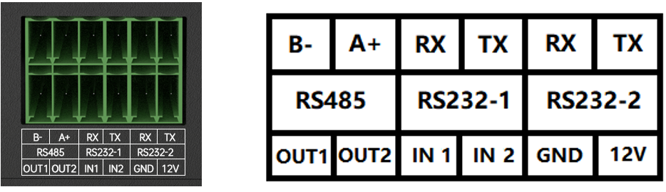
No.14
- Serial Port Introduction
For serial port usage, refer to: https://www.cnblogs.com/lizhuming/p/14044396.html
- GPIO Introduction
GPIO Input The two GPIO input channels adopt full isolation design, supporting normal operation with input voltage ranging from 3.3V to 12V. Logic of IN1/IN2:
- When the switch is set to H: The device receives high level for input high, and low level for input low.
- When the switch is set to L: The device receives low level for input high, and high level for input low.
GPIO Output
The two GPIO output channels are isolated by MOSFET with open-drain design. They support control levels from 3.3V to 24V, with a maximum sink current of 100mA.
- GPIO Function
No.19: 2.0mm 4-Pin Connector
RS485 — ttyS5RS232-1 — ttyS7RS232-2 — ttyS3IN1 — GPIO3_D0IN2 — GPIO3_D4OUT1 — GPIO4_B0OUT2 — GPIO4_B2External pull-up resistors are required for OUT1/OUT2 to work properly.The output follows positive logic: OUT1 outputs high when GPIO4_B0 is set high, and outputs low when GPIO4_B0 is set low.
| image-2026-4-10_18-3-20-1.png | PIN | 功能 | 描述 | 备注 |
| 1 | 3.3V电源输出 | 可输出100mA | ||
| 2 | GPIO2_A2 | I3C1_SCL_M1/CAN1_RX_M0 /SPI0_CSN1_M1/UART5_RTSN_M2 /JTAG_TCK_M0/SAI3_LRCK_M3 /DSM_AUD_RP_M0/FSPI1_D2_M0 /SDMMC0_D2 / GPIO2_A2_d | 3.3V 电平 | |
| 3 | GPIO | I3C1_SDA_M1/CAN1_TX_M0 UART5_CTSN_M2/JTAG_TMS_M0 /SAI3_SDI_M3/DSM_AUD_RN_M0 /FSPI1_D3_M0/SDMMC0_D3/GPIO2_A3_d | 3.3V 电平 | |
| 4 | GND | 电源地 |
3.Debug Function
No.20: 2.0mm 3-Pin Connector
| image-2026-4-10_18-5-1-1.png | PIN | 功能 | 描述 | 备注 |
| 1 | RXD | Uart0 RXD , 波特率1500000 ,Debug用 | 3.3V 电平 | |
| 2 | TXD | Uart0 TXD 波特率1500000 ,Debug用 | 3.3V 电平 | |
| 3 | GND | 电源地 | 3.3V 电平 |
4.Camera MIPI CSI
No.23: 0.5mm 24-pin connector
| PIN | Function | Description | |
|---|---|---|---|
| image-2026-4-10_18-6-5-1.png | 1 | SDA | I2C4_SDA_M3_MIPI_CAM0 |
| 2 | SCL | I2C4_SCL_M3_MIPI_CAM0 | |
| 3 | GND | Ground | |
| 4 | CAM0_PEN | GPIO3_C7_d, Camera power enable, active high | |
| 5 | CAM0_PEN | GPIO3_D5, Camera reset, active low | |
| 6 | GND | Ground | |
| 7 | CSI0_RX_CLKN | MIPI camera differential clock CLKN | |
| 8 | CSI0_RX_CLKP | MIPI camera differential clock CLKP | |
| 9 | GND | Ground | |
| 10 | MCLK | Reference clock MCLK | |
| 11 | GND | Ground | |
| 12 | CSI0_RX_D0N | MIPI camera differential data D0N | |
| 13 | CSI0_RX_D0P | MIPI camera differential data D0P | |
| 14 | CSI0_RX_D1N | MIPI camera differential data D1N | |
| 15 | CSI0_RX_D1P | MIPI camera differential data D1P | |
| 16 | GND | Ground | |
| 17 | CSI0_RX_D2N | MIPI camera differential data D2N | |
| 18 | CSI0_RX_D2P | MIPI camera differential data D2P | |
| 19 | CSI0_RX_D3N | MIPI camera differential data D3N | |
| 20 | CSI0_RX_D3P | MIPI camera differential data D3P | |
| 21 | GND | Ground | |
| 22 | CAM3_3V3 | 3.3V power output for camera, 500mA | |
| 23 | CAM3_3V3 | 3.3V power output for camera | |
| 24 | CAM3_3V3 | 3.3V power output for camera |
5. LCD MIPI DSI
No.24: 0.5mm 40-Pin Connector
| PIN | Function | Description | |
|---|---|---|---|
| image-2026-4-10_18-7-38-1.png | 1 | NC | No Connection |
| 2 | LCD_VCC | LCD power supply | |
| 3 | LCD_VCC | LCD power supply | |
| 4 | GND | Ground | |
| 5 | LCD_RST | LCD reset | |
| 6 | NC | No Connection | |
| 7 | GND | Ground | |
| 8 | DSI_TX_D0N | LCD MIPI differential data D0N | |
| 9 | DSI_TX_D0P | LCD MIPI differential data D0P | |
| 10 | GND | Ground | |
| 11 | DSI_TX_D1N | LCD MIPI differential data D1N | |
| 12 | DSI_TX_D1P | LCD MIPI differential data D1P | |
| 13 | GND | Ground | |
| 14 | DSI_TX_CLKN | LCD MIPI differential clock CLKN | |
| 15 | DSI_TX_CLKP | LCD MIPI differential clock CLKP | |
| 16 | GND | Ground | |
| 17 | DSI_TX_D2N | LCD MIPI differential data D2N | |
| 18 | DSI_TX_D2P | LCD MIPI differential data D2P | |
| 19 | GND | Ground | |
| 20 | DSI_TX_D3N | LCD MIPI differential data D3N | |
| 21 | DSI_TX_D3P | LCD MIPI differential data D3P | |
| 22 | GND | Ground | |
| 23-24 | TP_VCC | Touch panel 3.3V power output, 100mA | |
| 25 | GND | Ground | |
| 26 | SDA_TP | Touch I2C0_SDA_M1_TP | |
| 27 | SCL_TP | Touch I2C0_SCL_M1_TP | |
| 28 | RES_TP | Touch panel reset | |
| 29 | INT_TP | Touch panel interrupt | |
| 30 | GND | Ground | |
| 31-32 | LCD_BL- | Backlight negative terminal | |
| 33-38 | NC | No Connection | |
| 39-40 | LCD_BL+ | Backlight positive terminal, 18V-28V, 200mA |