RM182X Hardware Specification
1. Product Overview
RM182XMC0 (including RM1820MC0 and RM1828MC0) is a high-performance AI compute co-processor module supporting 3B / 7B large models (RM1820MC0 supports 3B, RM1828MC0 supports 7B), suitable for AI inference and machine vision applications — especially AI-related use cases.
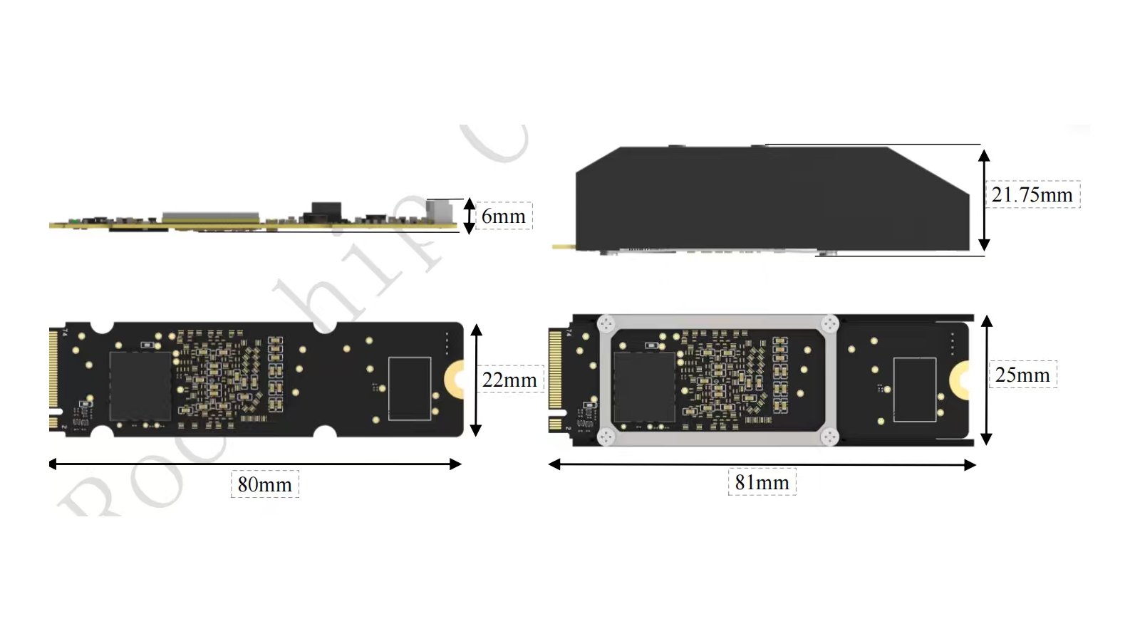
The module uses an M.2 Key M gold-finger connector and measures 22mm × 80mm. Customers only need to design a simple carrier board to integrate the module into edge or embedded devices for fast development.
2. Module Features
- RK182X delivers 20TOPS@INT8, supporting INT4 / INT8 / INT16 / FP8 / FP16 / BF16 arithmetic — widely used in AI inference and machine vision.
- RK182X embeds high-bandwidth on-chip DRAM:
- RK1820: 2.5GB
- RK1828: 5GB
- Currently supported models: Qwen 2.5 0.5B, Qwen 2.5 1.5B, Qwen 2.5 3B, Qwen 3 0.6B, Qwen 3 1.7B, FastVLM, MobilnetV1, MobilnetV2, Resnet50V2, yolov5s, yolov6s, yolov8s
- Software support: PC-side development kit (RKNN3 Toolkit), on-device runtime API (RKNN3 Runtime), and model conversion/deployment examples (RKNN3 Model Zoo).
3. Specifications
Module Basic Specification
| Item | Specification |
|---|---|
| SOC | Rockchip RK182X |
| CPU | 3-core RISC-V: SRV, VRV0 and VRV1 |
| SRV implements RV64GCB ISA; VRV0 and VRV1 implement RV64GCBV ISA | |
| All cores have 32KB L1 I-Cache, 32KB L1 D-Cache and 128KB L2 cache | |
| VRV0 and VRV1 additionally integrate a 128-bit vector unit | |
| NPU | 20TOPS@INT8 |
| Supports INT4 / INT8 / INT16 / FP8 / FP16 / BF16 arithmetic | |
| RAM | RK182X embedded high-bandwidth DRAM |
| RK1820: 2.5GB | RK1828: 5GB | |
| Hundreds of GB of bandwidth | |
| ROM | eMMC 32GB (OPTION) |
| High-speed expansion | 1× PCIe0, supports both EP and RC modes, supports PCIe EP boot |
| Power | 12V/3A (dedicated header on carrier board), 3.3V/3W (M.2 socket on carrier board) |
| Module interface | M.2 Key M Connector |
| Module dimensions | 22mm × 80mm |
| Operating environment | -10℃ ~ 55℃ |
| Software support | RKNN3 Toolkit, RKNN3 Runtime, RKNN3 Model Zoo, etc. |
JPEG Encode
| Item | Specification |
|---|---|
| Standard | Baseline (DCT sequential) |
| File format | JPEG File Interchange Format 1.02 |
| Image size | From 16×16 up to 65520×65520 |
| Color formats | YUV400 / YUV420 / YUV422 / YUV444 |
JPEG Decode
| Item | Specification |
|---|---|
| Standard | Baseline (DCT sequential) |
| File format | JPEG File Interchange Format 1.02 |
| Image size | From 48×48 up to 65520×65520 |
| Color formats | YUV400 / YUV420 / YUV422 / YUV440 / YUV411 / YUV444 / RG888 / RGB565 |
4. Power / Performance Parameters
Input tokens: 128
| Model | Mode | TTFT (ms) | TPS (tokens/s) | Power |
|---|---|---|---|---|
| Qwen2.5 3B | Power-save | 144.455 | 54.537 | Avg: 5.35W Peak: 15.14W |
| Qwen2.5 3B | Standard | 96.05 | 77.945 | Avg: 7.2W Peak: 24.86W |
| Qwen2.5 7B | Power-save | 288.255 | 35.044 | Avg: 7.02W Peak: 16.11W |
| Qwen2.5 7B | Standard | 186.435 | 51.476 | Avg: 10.4W Peak: 27.28W |
5. Module Power Supply
Besides the 3.3V provided by the carrier board through the M.2 interface, the module requires an additional 12V supply.
| Rail | Provided by | Specification |
|---|---|---|
| 12V | Dedicated header on carrier board | 12V / 3A |
| 3.3V | M.2 socket on carrier board | 3.3V / 3W |
Supplying only 3.3V through the M.2 socket will not drive the module. The carrier board must implement a dedicated 12V/3A power path.
6. Module Block Diagram and HOST Connection
 3.3V ──┐
        ├─► BUCK / LDO ──► RK182X Power
 12V ──┘

 RK182X ──► PCIe0 (EP / RC)  ◄──► HOST PCIe RC / EP
        ──► NPOR / RST
        ──► CLKREQ  ──────────► PCIe CLKREQn
        ──► PWM     ──────────► FAN_CTRL (PWM_CH6_M0)
        ──► GPIO    ──────────► FAN_SPEED (PWM_CH7_M0)
        ──► 24MHz OSC
Module-side signals:
| Signal | Description |
|---|---|
3.3V_IN | 3.3V input from the M.2 socket |
VCC_IN | 12V input from the dedicated carrier-board header |
PCIE0_PERSTN_M0 | PCIe global reset |
PCIE0_CLKREQN_M0 | PCIe reference clock request |
PCIE0_WAKEN_M0 | PCIe wake |
FAN_CTRL (PWM_CH6_M0) | Fan speed control |
FAN_SPEED (PWM_CH7_M0) | Fan speed detection |
RESETN_IN | Module reset input |
PCIe0 EP | Main HOST communication interface (PCIe 2.1 1lane) |
7. Module Dimensions
| Dimension | Value |
|---|---|
| Module length | 80mm |
| Module width | 22mm |
| Module thickness | 6mm |
| Total length incl. gold finger | 81mm |
| Structural reference width | 25mm |
| Key notch position | 21.75mm |
8. Ordering Information
| Ordering model | Interface | Description |
|---|---|---|
| RM1820MC0 | M.2 Key M, PCIe2.1 | Chip RK1820, supports 3B large models |
| RM1828MC0 | M.2 Key M, PCIe2.1 | Chip RK1828, supports 7B large models |
For 3B-class models only, RM1820MC0 is the cost-effective choice. If you need 7B-class models (e.g. Qwen2.5 7B), choose RM1828MC0 with 5GB on-chip DRAM.